Materials Research Center for Element Strategy, Tokyo Institute of Technology.
MAJOR ACHIEVEMENT RESEARCH
Major Achievements in Research
Discovery of High-Tc Iron-Based Superconductors, and Creation of Transparent Oxide Electronics and Materials Science of Electrides
Dr. Hideo Hosono has concentrated on the cultivation of electronic functions in inorganic materials over the past 2 decades and created several innovative materials, some of which have opened novel and large academic fields and/or led to large industrial applications. His approach is to combine physical measurements with unique material choices based on his chemical intuition. He has published ~1,000 original papers (h-index 127), 5 books in English, ~90 registered international patents on these subjects, and has received many scientific prizes including the Imperial Prize and Japan Academy Prize, the highest academic honors in Japan (each year a single Imperial Prize is awarded in the natural science sector to the researcher with greatest research achievement) and several highest prizes from the academic societies such as Materials Research Society (MRS), Society for Information Display(SID) and American Physical Society. In 2016, the Japan Prize, the highest international prize endorsed by the Japanese Government, was awarded to him for “Creation of unconventional inorganic materials with novel electronic functions based on nano-structure engineering”. The impact of his research not only developed new areas in materials science but led to large industrial application. The highlights of his research achievements are summarized as follows:
1. Discovery of High-Tc Iron-Based Superconductors
Magnetic elements with large magnetic moments, such as iron, were widely believed to be harmful for the emergence of superconductivity because static magnetic ordering competes with the dynamic formation of electron pairs (so called Cooper pairs). It was thus transformative when Dr. Hosono discovered the iron-based superconductors (IBSCs) LaFeOP (Tc=4K, JACS 2006) and LaFeAsO1-xFx (Tc=26K, JACS, 2008), in the course of his exploration of magnetic analogues of the p-type transparent semiconductors LaCuOCh(Ch=S,Se) with similar crystal structures. This discovery fired extensive research globally, leading to the publication of more than ~several ten thousand of papers in the last decade. His JACS 2008 paper became the most cited paper published in 2008 in all disciplines, and the discovery of IBSCs was selected as breakthrough of the year by the Science Magazine. Nature magazine’s feature “High Temperature Superconductivity (Vol.475, pp.280) highlighted ten achievements in the field, two of which were the discovery of new superconductors: the high Tc cuprates in 1986 by Bednorz and Muller and high Tc iron-based superconductors in 2008 by Hosono et al.
His group has been leading the materials research on IBSCs since their discovery.
They achieved first fabrication of epitaxial thin films of IBSCs and their
use in the fabrication of a superconducting quantum interference device
(Supercond. Sci. Technol. 2010). His group also elucidated how the nature of the grain boundaries in IBSCs
leads 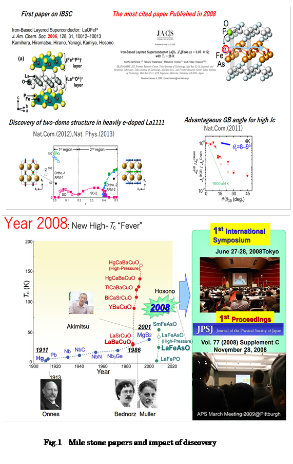 advantages for wire fabrication, especially when compared with the cuprates
(Nat.Comm. 2011). This finding encouraged the researchers of superconducting
wires, and the critical current density of IBSC wires prepared by conventional
methods has reached the performance level needed for practical applications
(See A review by Hosono et al., Materials Today 2018).
advantages for wire fabrication, especially when compared with the cuprates
(Nat.Comm. 2011). This finding encouraged the researchers of superconducting
wires, and the critical current density of IBSC wires prepared by conventional
methods has reached the performance level needed for practical applications
(See A review by Hosono et al., Materials Today 2018).
Recently, he uncovered new phenomena in the Tc vs. e-doping behavior of
LaFeAsO following a unique chemical idea: previously unobtainable e-doping levels were achieved by replacing O2- with H- ion using high pressure synthesis techniques (Nat.Comm. 2012). This approach revealed that the shape of the Tc-dome is not the simple
peak expected but instead has a double-dome structure resulting from two
distinct parent materials with different magnetic structures (Nat.Phys.
2014, PNAS, 2017). This finding provides an important clue (Phys.Rev. B. 2016) for the elucidation
of the mechanism for high Tc superconductivity in IBSCs. I think this success beautifully illustrates the productivity of Hosono’s
favorite approach of combining a chemical idea with a physical method.
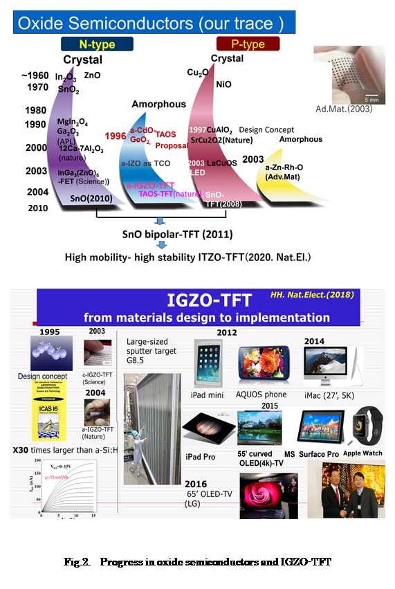
2. Creation of Transparent Oxide Electronics
Most of transparent oxides, such as glass and alumina, are insulators. The few exceptions to this rule are known as transparent conducting oxides (TCOs). The representative examples are In2O3 doped with Sn4+ and ZnO doped with Al. Although TCOs are widely used as transparent electrodes, their application as transparent semiconductors is impossible because tuning the Fermi level with a biasing voltage is difficult in these materials. In addition, no p-type transparent oxide material was reported when Hosono entered the field. This was a large obstacle to establishing transparent oxide-based electronics, because the p-n junction is a key element for the active functionality of semiconductors.
Hosono created new materials that led to the solution of the above issues. First was the invention of transparent amorphous oxide semiconductors (TAOS) with large electron mobility comparable to that of polycrystalline analogues. He designed TAOS based on a simple consideration of the orbital constitution for the conduction band minimum (CBM) in the post-transition metal cations. Since the overlap between the s-orbitals of adjacent metal cations (through intervening oxygen atoms) is large and insensitive to the structural randomness, he deduced that amorphous versions of these post-transition metal oxides could retain large electron mobility. This idea was proposed in 1996 along with several concrete materials (J.Non-Cryst.Sol. 1996, 2006) and was later demonstrated in the lab using various spectroscopic techniques combined with cluster calculations (Phys. Rev. B,2002). In 2003-4, he fabricated thin film transistors (TFTs) using InGaZnOx (IGZO), which can be prepared as a TAOS, and reported that IGZO-TFTs have large electron mobilities that are an order of magnitude higher than that of amorphous Si:H. These publications on crystalline (Science,2003) and amorphous IGZO-TFTs (Nature,2004) strongly stimulated the display and amorphous semiconductor communities, and extensive research on oxide TFTs started rapidly. As a result, these two papers became the most cited publications (2100 for Science, 5300 for Nature) regarding oxide semiconductors. The citation count of a series of his patents has risen to ~30,000 (Google Scholar), the largest number in this field. IGZO-TFTs are now practically used as the backplane to drive high-resolution and energy-saving LCD panels, and OLED-TVs. The most visible product with IGZO-backplane is large-sized (55&65’) OLED-TVs by LG display, which are now rapidly growing in market. The president (Sang-Deog Yeo) of LGD said these OLED TVs could not realize without amorphous IGZO-TFTs. The 3 papers on IGZO-TFTs were ranked in world top 10 in the most cited paper in parents (National Institute of Science and Technology Policy). Recently, he described a brief story of IGZO-TFT invention in Nature Electronics upon request (Nature Electro. 2018).
Hosono’s second major contribution to this field is the realization of p-type oxide semiconductors. In 1997, the first transparent p-type oxide semiconductors CuAlO2 was reported along with a chemical design concept (Nature,1997). Subsequently, a series of new transparent p-type semiconductors using Cu+-bearing layered oxides, such as SrCu2O2 and LaCuOS, and pn-junction devices were fabricated employing these materials. He also succeeded in finding bipolar oxide semiconductors similar to Si using CuInO2.
The most important work on this subject achieved by Hosono is the realization of the first p-channel TFT using SnO (Appl. Phys. Lett. 2008). Although more than 10 p-type oxide semiconductors based on Cu+ were reported, there was no material which worked as active layers in p-channel TFTs until the appearance of the SnO-TFT in 2008. Subsequently, he demonstrated the first C-MOS operation of a SnO-TFT, which is a mile stone in the oxide semiconductors field (Adv. Mater. 2011).
Recently, he created new transparent semiconductors based on novel materials
design concepts: bipolar ZrOS utilizing orbital symmetry(JACS 2017), transparent p-type semiconductor with large mobility, Cu-Sn-I, which
can be fabricated by solution process (Adv.Mater.2018), and ZnO-SiO2 with exceptional properties (Adv.Ele.Mat.2017).
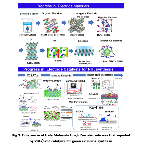
3. Materials Science of Electrides
An electride
is a crystal in which electrons serve as anions. The electride concept and the
first electride material were reported in 1983 by J. L. Dye. Despite the potential inherent in their
remarkable electronic structures, electrides prepared subsequently (restricted to
organic materials) are so chemically and thermally unstable that almost no
physical properties had been measured. In 2003, Hosono succeeded in
synthesizing the first RT stable electride (Science, 2003), employing 12CaO·7Al2O3 (a constituent of
alumina cement, abbreviated hereafter as C12A7). In his design process, he
focused on the unique crystal structure of C12A7. Here, positively charged sub-nm-sized cages
are connected through shared oxide monolayers to form a 3D-structure, and O2-
ions are loosely bound as counter anions to maintain electro-neutrality. Hosono was able to exchange these loosely
bound O2- ions with electrons. The resulting material may be
regarded as an electride (C12A7:e) and exhibits a metal-insulator transition (Nano
Letters, 2007). Furthermore, when metallic C12A7:e is cooled down, it was found
to display superconductivity! (JACS,2007). Surprisingly, the electronic structure of
C12A7:e is similar to that of the superconducting high-pressure phase of
lithium metal (Phil.Trans.R.Soc.A, 2015). Such a discovery demonstrated the
hidden potential of abundant elements and led to the establishment of a Japan
Science& Technology Policy “Element Strategy Initiative”.
After considering the unique properties of C12A7:e—its very low
work function(2.4eV) but strong chemical & thermal stability—Hosono
discovered that Ru-loaded C12A7:e showed high catalytic activity for ammonia
synthesis at ambient pressure (Nat. Chem., 2012, Nat.Com. 2015). Furthermore,
he extended the concept of electride to intermetallics and found a series
of new electride materials and their high catalytic activity for NH3 synthesis (Nature Catal. 2018). As a result, a company aiming at industrial application of his invention
to on-site NH3 synthesis was established in 2017 by sponsorship of a Governmental fund,
UMI, and Ajimotomo, the largest food company in Japan.
In addition, he extended the electride concept to 2D-materials in which
anionic electrons occupy spaces between cationic slab layers and found
Ca2N to be one such 2D electride material, formulated as (Ca2+)2(N3-)(e-), in 2013 (Nature, 2013). Since no impurity scattering contributes to their electron transport, 2D
electride materials have extraordinarily large conductivities compared
with conventional metals. In fact, the electrical conductivity of Ca2N exceeds that of metallic Ca. Two D electride materials may be viewed
as bulk analogues to the 2D-electron gases which occur at clean hetero-interfaces
between semiconductors such as GaAs/AlGaAs. Subsequently, he screened candidates
for 2D-electrides by utilizing Materials informatics and found Y2C and Gd2C as a magnetic electride (PRX 2016, PRB 2017). Since then, research on
2D-electrides is booming up to now. Amorphous electrides were first created
as well by Hosono who fabricated C12A7:e glass by twin-roller technique
(Science 2011) and the thin films of amorphous (a-) C12A7:e by sputtering.
He found these a-C12A7:e has several unique properties; the bulk glass
transition temperature is dropped by ~150K just replacing ~3% of O2- by electrons (PNAS, 2017A) and the work function is 3.0eV, which is close
to metal Ca or Li but chemically stable and optical transparent. This unique
property was successfully applied to an electron-injection layer in OLEDs
and efficient inverted-type OLEDs were realized (PNAS, 2017B)